
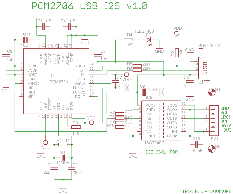
This module is converter from USB to I2S bus up to 48kHz sample frequency. It use circuit PCM2706 from Texas Instruments. It is connected in mode where send his output to signals in format of I2S bus. Analog part is completely unconnected similar to S/PDIF output which can't be used in this mode. I2S output is electrically isolated to prevent of ground loops and his troubles with noise and hum on the output.
Circuit PCM2706 is supplied from a VBUS signal on the USB bus. R2 allows computer to detect connected device to the USB bus. R5 and R6 are for eliminating of signal reflection to the cable. Voltage VDD 3.3V is generated by internal regulator. On the VBUS is connected LED indicating presence of voltage on the USB bus. About circuit are decoupling capacitors. Converter is in hardware mode and with pin FSEL is switched to the I2S output mode. I2S bus is on the pins FUNC0, FUNC1, FUNC2 and DOUT. Circuit is designed also for PCM2707 without any change.
I2S bus goes via resistors R7 to R10 on the digital isolator ISO7240C which isolates USB I2S bus from rest of DAC circuit. Isolating circuit is interesting that it allows connect from input and output side different supply voltage and with this make logical level conversion. For example LVTTL 3.3V to TTL 5V. Output side is supplied from a DAC board. Both sides have on the supply pins decoupling capacitors C9 and C10.
First I assembled USB-I2S converter IC1 and isolator IC2. First I soldered two pins in opposite corners and after check of right position I soldered rest pins with help of much flux and tube tin. I ride over pins with a soldering iron until all pins are nicely soldered. Possible jointed pins I suck with a solder wick. Next I continued with SMD resistors and capacitors. next I soldered connectors. I soldered LED after mounting of all boards in to the chassis for their right fit in to the hole. Board is inserted with socket ribbon SV1 to the pins on the DAC board and screwed with two M3 screws for good mechanical strenght while inserting USB connector.
Printed circuit board is designed doublesided with size 5x5cm because cheaper manufacturer price. Except crystal are all components from a bottom side because above board is mains connector. I ordered manufacturing of PCB at Seeed Studio. Required Gerber and Excellon files is possible to generate in a Free version of Eagle from documents which are available here.
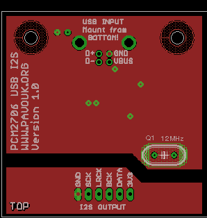
Top side view.
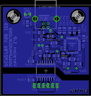
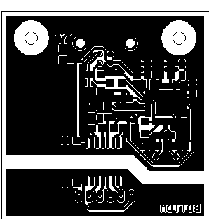
 Bottom side view.
Rear panel view.
Bottom side view.
Rear panel view.

Parts can be purchased for example at Farnell company. I used older revision of PCM2706 without letter "C". Newer revision has changed volume characteristics because a new Windows certification. Volume only works for analog output that on I2S output it is without volume change. In some operationg systems is possible to change volume. It means that it has software mixer which means distortion of samples which goes to the DAC. In this example I recommend to set volume on the maximum in a computer.
| name | value and type | quantity |
|---|---|---|
| C1, C2 | 22pF SMD1206 ceramic | 2x |
| C3-C8 | 1uF SMD1206 ceramic | 6x |
| C9, C10 | 100nF SMD1206 ceramic | 2x |
| C11 | 10uF tantal SMD size A | 1x |
| IC1 | PCM2706C (PCM2707C) | 1x |
| IC2 | ISO7240C | 1x |
| LED1 | LED yellow 2mm cylindrical | 1x |
| Q1 | Crystal 12MHz package HC49US low profile | 1x |
| R1 | 1M SMD1206 | 1x |
| R2-R4 | 1k5 SMD1206 | 3x |
| R5-R10 | 22R SMD1206 | 6x |
| SV1 | Ribbon socket 6 pins 10mm | 1x |
| X1 | USB type B to the PCB 90° | 1x |
Circuit works on the first power-up. USB chip support sample frequency up to 48kHz. Simple chip with higher sample frequencies now doesn't exists. For me it is not problem because now I have majority of records in CD quality.
-
 English
 Česky
Česky