
I found interesting integrated circuit from Texas Instruments production which creates lossless digital audio wireless link up to 48kHz sample frequency. Circuit has many applications like wireless substitution of S/PDIF cable, wireless headphones or speakers, USB soundcard etc. Circuit works in 2.4GHz band and use proprietary protocol which is tolerating to WiFi and Bluetooth. Because I haven't any experience with construction in high frequency area that I chosed project like challenge and I also used a new DAC PCM5102 and S/PDIF encoder DIT4096 which are also unknown to me.
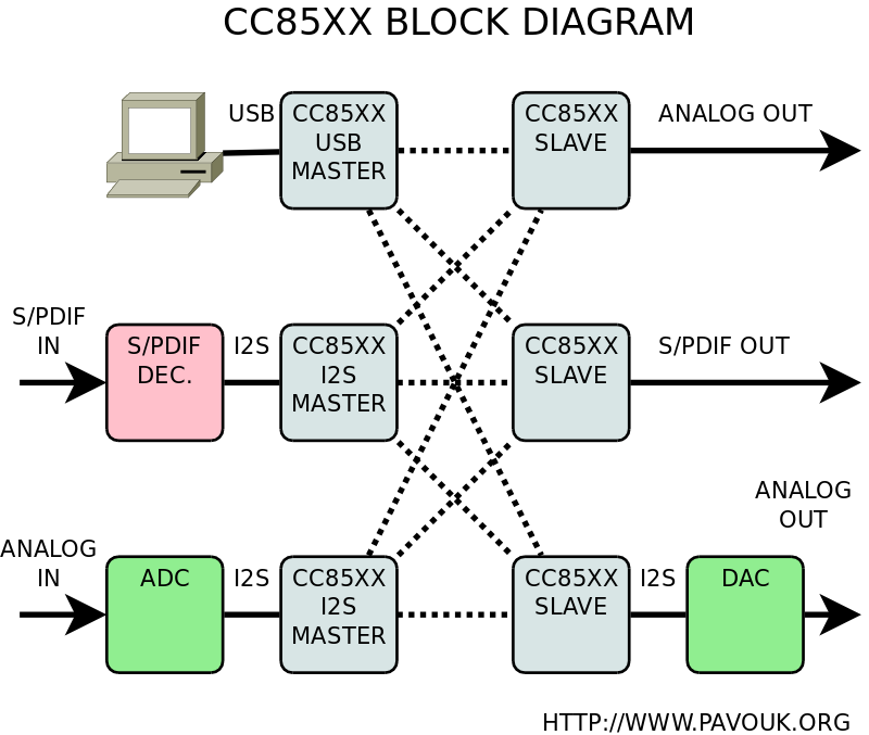
Block diagram show possibilities of use of boards in a various parts
of audio chain. It is possible to combine any inputs and outputs and we can
also simultaneously connect 4 slave devices to one master. If we want
to connect S/PDIF input to the master that we must use external decoder
like one of my decoders based on DIR9001 or CS8416 which are parts of
modular dac project.
Product line of digital wireless audio products includes now 4 circuits. Their differences are in this table:
| Name | Number of audio channels | USB support |
|---|---|---|
| CC8520 | 2 | NO |
| CC8521 | 2 | YES |
| CC8530 | 4 | NO |
| CC8531 | 4 | YES |
Chip includes processor part, many input-output pins, complete radio part and some versions support USB interface. Radio part use adaptive frequency hopping, forward error correction (FEC), buffering, retransmissions with transfer rates 5 or 2 Mbps. For transferring of more than two channels is needed to use embedded slight loss audio codec (SLAC) because there is not enough width of band. Technology use Master - Slave topology where we can connect up to 4 slave units to one master. When we use master in USB mode that circuit is visible like a standard USB soundcard in operating system and doesn't need any drivers. In this mode we can transfer from slave units HID events like volume regulation or stop and play buttons. Circuit has also I2C bus interface which can for example set volume in connected DAC. Circuits is programmed via SPI connector for example with help of CCDebugger from TI. For programming is not needed to know any programming language because firmware is created with help of PurePath Wireless Configurator. Circuit can be programmed many times. From time to time is published a new version of configurator with a new firmware with new features. Circuit allows to connect external amplifier CC2590 for longer distance with more power and better sensitivity. Audio data are in I2S format or one side (master) can be USB audio. master and slaves can be paired with button or automatically or with fixed network ID.
I designed Circuit and PCB universally that we can use them in these modes:
In USB master mode is board connected via USB cable where it is visible like standard USB soundcard with two audio channels. In I2S master mode is connected standard I2S signal to the board. For example when we want to transfer S/PDIF signal via air we must connect external S/PDIF decoder to the master because circuit doesn't include them. Board can be powered via +5V pin on the I2S connector or via USB connector. In slave mode we can board connect for example via his S/PDIF output to the some HiFi receiver and power it via USB connector or we can use I2S output and connect board with high-quality DAC. We can also use analog output from PCM5102 DAC and connect them with preamplifier or power amplifier. Better chip support modes of worse chips that for example we can use CC8521 instead of CC8520 but not in opposite. If we want to mount the board in to the some shielded box it is a good idea to disconnect internal PCB antenna and reconnect HF signal with R0 to external antenna via onboard SMA connector.
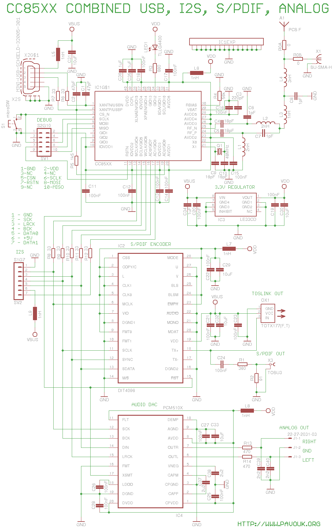
Heart of circuit is chip IC1 CC85XX. On pins 1 and 2 is connected USB input. Presence of device on USB bus is driven by resistor R5 from pin 19. On the pin 3 is connected push-button dedicated for pairing. This pin is also for chip-select on program interface. Pins 4, 5 and 6 are used for programming via DEBUG connector. On the pin 8 is present signal which resets S/PDIF encoder and blocks analog output of DAC when it is in reset state. Via pin 11 we can reset circuit from DEBUG connector. Pins 13 to 16 are dedicated for I2S bus. They can be input or output depending on programmed firmware image. On pin 17 is connected second I2S data signal for experiments with two additional audio channels. On pins 21 and 22 is connected crystal oscillating on 48MHz fundamental frequency. It is not possible to use crystals which oscillate on third order frequency. On pins 24 and 25 is symmetrical radio input/output. To them is connected balun which match the output to the unbalanced antenna with 50 ohm impedance. On pin 34 is connected LED signalling various operation states like not available signal, pairing or power-on.There is also many blocking capacitors in accordance to the recommendation.
Board is powered from +5V but because major of circuits requries 3.3V that there is on the board IC3 LE33 low-drop voltage regulator. Around them are also blocking capacitors.
On the I2S output is wired S/PDIF encoder DIT4096 which is configured in hardware mode with pins for accepting data format from wireless chip. His output goes to the optical transmitter OX1 and paralelly via capacitor C24 to the resistor divider R1 and R2 which match the output for around 75 ohm and voltage level about 1V.
Parallely to them on the I2S bus is connected DAC PCM5102. It is relatively new type of delta/sigma convertor which includes power source of negative voltage and thanks to this it can have analog output in level 2.1V RMS line-out without use of coupling capacitor. It can allow to select type of interpolation filter normal (FIR) or with low-latency (IIR). IIR filter has advantage of suppression of preringing which is ugly thing on which is human ear very sensitive and it is one of main reason why sound from delta/sigma DACs is evaluated worse than sound from R/2R type DACs without oversampling. Around them are only few capacitors on power pins and output filter from R13, C39 and R14, C40 which has declination for 3dB at 153kHz. It is also possible to use DACs PCM5100 or PCM5101 which have a little worse parameters.
Assembling of board is very hard. Circuit IC1 in pinless QFN40 package can't be assembled without oven or hot air and solder paste. I had access to oven for PCB that I baked boards with assembled IC1 and also IC2 and IC4 on some boards. Rest of parts I assembled manually. Unfortunately thanks to a new paste was soldering not much good and I had to all pins resolder manually with help of flux and tin. For this work is really needed strong magnifying glass because for normal eyes are pins too close. Luckily all my four boards was succesfully soldered.
After assembling of chips we continue with sequential assembling of SMD resistors and next capacitors. It is pretty hard, because parts are in 0603 package and I had 0.6mm tube tin and relatively big soldering iron. But with precise work it can be succesfully soldered. Next we assemble regulator IC3 and next crystal, connectors and push-button. It is not needed to assemble all parts when we don't need for example S/PDIF output or analog output that we don't assemble relevant chip and all parts around them. Not populated parts are visible on photos.
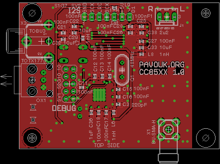
Printed circuit board is double-sided and it is designed to fit in plastic box U-KP50 (Z70). I tried to design it with accent to right part positioning from a noise and shield view. On the PCB is also integrated inverse F type antenna for 2.4GHz band. Place for crystal is for classic enclosure HC-49 but I didn't found them for 48MHz frequency. I ordered manufacturing of PCB at Seeed Studio.
Closed case with external antenna.
 Look to the open box.
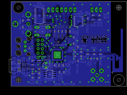
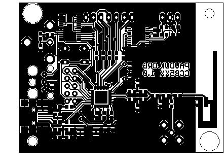
 Look on the bottom side of fully planted board with internal antenna.
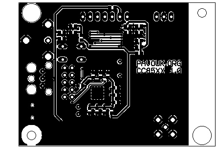
 Look on the bottom side of board without S/PDIF decoder and DAC with external antenna.
 Look from a top side on the board without S/PDIF decoder and DAC with external antenna.

Parts can be purchased for example at Farnell company. Some of SMD coils was available only at 0402 size. I used standard SMA connector but most of antennas for 2.4GHz band are available with reverse SMA connector that I used a small piece of wire inserted between both connectors. Be careful with selection of crystal! It must oscillate at 48MHz on fundamental frequency. Usually are available crystals oscillating at 3rd order frequency which need modified oscillator circuit. In this circuit their oscillating at 16MHz what we don't want.
| name | value and type | quantity |
|---|---|---|
| C1, C2 | 47pF SMD0603 ceramic | 2x |
| C3 | 220pF SMD0603 ceramic | 1x |
| C4, C5 | 18pF SMD0603 ceramic | 2x |
| C6-C8 | 1pF SMD0603 ceramic | 3x |
| C9, C10 | 16pF SMD0603 ceramic | 2x |
| C11-C28 | 100nF SMD0603 ceramic | 18x |
| C29-C33 | 10uF SMD0603 ceramic | 5x |
| C34-C36 | 1uF SMD0603 ceramic | 3x |
| C37, C38 | 2u2 SMD0603 ceramic | 2x |
| C39, C40 | 2n2 SMD0603 ceramic | 2x |
| IC1 | CC8520 (CC8521, CC8530, CC8531) by needs | 1x |
| IC2 | DIT4096 | 1x |
| IC3 | LE33CD SOIC8 | 1x |
| IC4 | PCM5102 (PCM5100, PCM5101) | 1x |
| J1 | Molex 3pin 90° | 1x |
| L1, L2 | 2nH SMD0603 | 2x |
| L3 | 1nH SMD0603 | 1x |
| L4 | 3nH SMD0603 | 1x |
| L5-L9 | 1nH SMD0603 ferrite bead (FB) | 5x |
| LED1 | Green 3mm 2mA | 1x |
| OX1 | TOTX177(F,T) Toshiba, GP1FAV31TK0F SHARP | 1x |
| Q1 | Crystal 48MHz fundamental frequency | 1x |
| R0 | 0R SMD0603 | 1x |
| R1 | 360R SMD0603 | 1x |
| R2 | 91R SMD0603 | 1x |
| R3 | 680R SMD0603 | 1x |
| R4 | 56k SMD0603 | 1x |
| R5 | 1k5 SMD0603 | 1x |
| R6-R12 | 33R SMD0603 | 7x |
| R13, R14 | 470R SMD0603 | 2x |
| S1 | push button 6x6mm | 1x |
| SV1 | Jumper ribbon 2x5 pins | 1x |
| SV2 | Jumper ribbon 1x7 pins | 1x |
| X1 | SMA connector to the PCB 90° | 1x |
| X2 | miniUSB socket SMD | 1x |
| X3 | cinch socket TOBU3 | 1x |
Files for PurePath Wireless Configurator.
Complete project was harder than all my previous projects. I teached many things when I designed High-frequency PCB and I tried design of circuit with CC85XX, DIT4096 and PCM5102 chips and also verified usability of complete solution. Boards have a smaller coverage than is written in tests. I think that it can be caused by not precisely designed wires from a HF view. Range with PCB antennas is about 5 meters in a room. To the neighbour room signal have drop-outs. Boards with external antennas have coverage to the neighbour room or to the next floor. From one end of house to the opposite end signal has outages. In future I will try to measure boards with a spectrum analyser. Transfer of digital audio is perfect. When the interference is partial that works error correction which provides error-free transfer of digital audio. When the interference is huge or signal is weak, that error correction is unsufficient and in audio are drop-outs. When the signal is very weak that audio line is disconnected. When the conditions are better that link is immediately reconnected and audio continue playing. Operation status is signalized with LED.
-
 English
 Česky
Česky