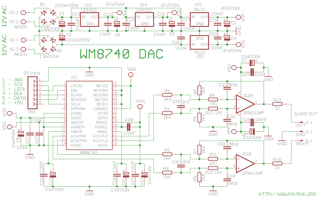
I had some time at home hidden circuit WM8740 and I get idea to create DAC with them. It is high performance DAC with oversampling, delta-sigma architecture and maximum sample frequency 192kHz/24bit. It has balanced voltage output. It is connected to high-quality operational amplifier which has low-pass filter function and buffer with single-ended output. Board also includes complete power part of circuit except transformer.
In supply part I used two bridge rectifiers similar to other my dac boards. For supplying of analog and digital part of dac I used low-drop voltage regulators LE50. For supplying of operating amplifier I used common 78L12 and 79L12 voltage regulators. We must use transformer with two secondary windings with 12 to 15V. Winding for positive supply branch AC1 can be paralelly connected to S/PDIF decoder when we haven't individual winding for them. All voltage regulators are properly blocked with ceramic capacitors 100nF and on the output filtered with electrolytic capacitors 47uF/16V. DAC and operational amplifier have also blocked all supply pins according to datasheet with ceramic capacitors 100nF and small electrolytic capacitors 10uF/16V.
DAC is set to HARDWARE mode with pin MODE. It means, that settings are changed with setting right pins to LOG 0 or 1. With pins CSBIWO and ML/I2S is configured data format for I2S/24bit. This format is most common and is supported on all S/PDIF decoders and USB soundcards with I2S output.
DAC has balanced voltage outputs. To them is connected 2nd low-pass filter with dual operational amplifier with very low distortion OPA2134. This amplifier simultaneously converts balanced output to unbalanced. Schematics of filter is adopted from AK4396 datasheet. On the output is connected small resistor which could prevent oscillations when not ideal load is connected. The output doesn't need coupling capacitor, when parts are properly selected. I measured DC-offset voltage 1.9mV on one channel and zero on another.
We assemble board from smallest parts to biggest. We begin with DAC IC1 because later it would be hard to install them. Next we continue with SMD capacitors and resistors. Later we continue from a top side with IC2 socket, voltage regulators IC3 to IC6, rectifiers, connectors and big electrolytic capacitors C1 and C2. With accurate assembling circuit could work on the first power-on. Specially we must be care with orientation of integrated circuits and polarity of all electrolytic capacitors.
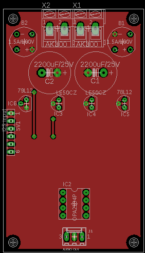
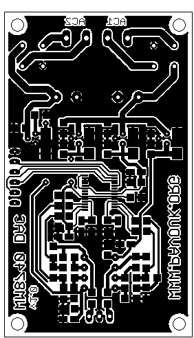
Top side
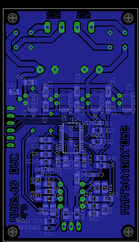
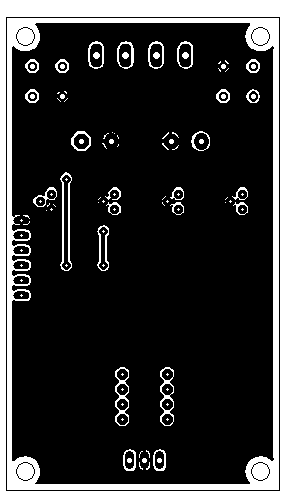
 Bottom side
I designed double-sided printed circuit board with ground planes. However it can be created single-sided with two wire junctions on a top side. In this case we can create them by photographics way in amateur conditions at home. I had left create like a prototype at MEV company. Professional double-sided board is about six times more expensive in a single piece manufacturing, but it looks much better and work with him is better too.
Top side of board version 1.0
 PDF format
Eagle6 format
PDF format
Eagle6 format
Bottom side of board version 1.0
 PDF format
Eagle6 format
PDF format
Eagle6 format


SMD capacitors and resistors have size 1206 that they can be easily soldered. DAC and operational amplifier are not common available in my local store. I bought them at Farnell company. Electrolytic capacitors are best types with low ESR. Rest components are commonly available. We use main transformer with two secondary windings 12V. Best types are with toroidal or CI core.
| name | value and type | quantity |
|---|---|---|
| B1, B2 | Bridge rectifier 1.5A/100V | 2x |
| C1, C2 | 2200uF/25V low ESR electrolytic RM5 | 2x |
| C3-C6 | 47uF/16V low ESR SMD tantal size C | 4x |
| C7-C12 | 10uF/16V low ESR SMD tantal size A | 6x |
| C13-C28 | 100nF SMD1206 ceramic | 16x |
| C29, C30 | 3n3 SMD1206 ceramic | 2x |
| C31-C34 | 680pF SMD1206 ceramic | 4x |
| IC1 | WM8740 | 1x |
| IC2 | OPA2134PA DIL8 | 1x |
| IC3, IC4 | LE50 TO92 | 2x |
| IC5 | 78L12 TO92 | 1x |
| IC6 | 79L12 TO92 | 1x |
| J1 | Molex 3pin | 1x |
| R1-R8 | 2k4 SMD1206 | 8x |
| R9-R12 | 150R SMD1206 | 4x |
| R13, R14 | 10R SMD1206 | 2x |
| SV1 | Jumper ribbon 6 pins | 1x |
| X1, X2 | Frame terminal AK300/2 | 2x |
| Patice IC2 | Precise DIL8 socket | 1x |
DAC works perfectly on the first connection. His sound is strain with balanced characteristics without any interference. I checked the output waveform with a oscilloscope and it looks exactly to my expectations for DAC with oversampling and delta-sigma modulation. His response to unit impulse or square wave has preringing and postringing. This dac have another filter which eliminate preringing which is good for sound, but it is available only in software mode. I tested two variants with System clock 128FS and 256FS. In 256FS mode output has much bigger pre and postringing. In 128FS mode it is much better. In datasheet is information, that in this mode is first stage of digital filter bypassed. 128FS mode also supports all common sample frequencies from 44.1kHz/16bit to 192kHz/24bit and is also supported on USB soundcards with I2S output. I recommend to set system clock to 128FS on S/PDIF decoders or other data sources with I2S output. Against to R-2R DACs without oversampling and without output filter is sound on high frequencies a fewer clear but it is a less stress. It is probably very subjective. His sound is excellent and it is only about personal preferences and money which DAC to select. Also price of manufacturing of this board is about five times cheaper than price of board with two PCM1704 DACs.
-
 English
 Česky
Česky