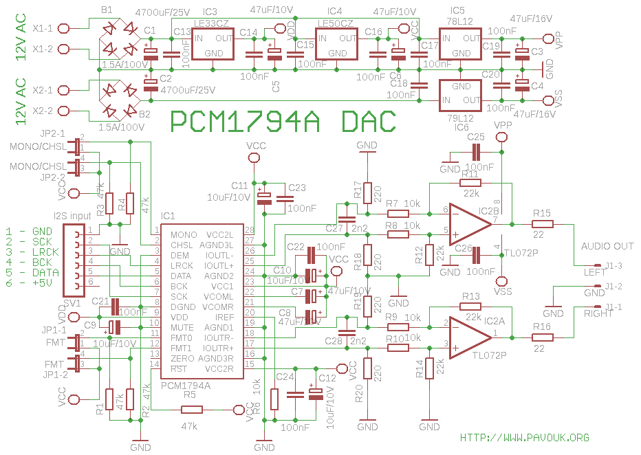
There is DAC with integrated circuit PCM1794A. It is one of execellent audio DACs from Burr Brown (Texas Instruments). It has 24-bit resolution, 192kHz sample frequency, 8x oversampling digital filter, differential current output and SNR 127dB.
Circuit includes power supply, DAC and operational amplifier.
For power supply is needed transformer with two individual secondary 12V windings. If you want to supply from transformer S/PDIF decoder and transformer doesn't have third separated winding, we must connect supply input of decoder parallel to winding for positive branch otherwise there will be short circuit. Voltage is rectified by B1 and B2 bridges and goes through filter and decoupling capacitors to low-drop regulators IC3 and IC4 which feeds analog and digital part of DAC. IC5 and IC6 regulates voltage +12V and -12V for operational amplifier. All supply inputs of DAC are properly decoupled with capacitors.
DAC PCM1794A works with data from standard I2S bus. In addition to it use signal SCK - System clock, which needs for proper function and oversampling. Input data format, output type and characterics of digital filter is selected with jumpers. Circuit includes internal reset with external pull-up resistor R5. Output is current differential. For conversion to voltage output I use resistors R17 to R20. They should be high quality carbon resistors. Behind these resistors we can theoretically take out symmetrical output to high impedance input of preamplifier. C27 and C28 are used for limit of high frequencies out of audible sound.
For getting of single-ended output with average value at zero I used low-noise operating amplifier TL072. Gain is about two. I inspired by original circuit because I am not specialist for operating amplifiers. In original circuit are used operating amplifiers for conversion of current to voltage output too. I used only resistors which are better and simpler. In quiet outputs have zero voltage, that theoretically we don't need coupling capacitors. On one output was voltage about 12mV and on another 2.6mV. It can be better by selecting value of resistors.
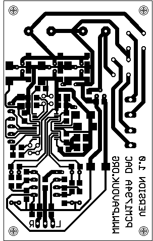
Parts are placed from smaller to bigger. I begin with IC1. Method of his placing is same like on S/PDIF decoder. Next I continued with SMD resistors and capacitors. Next I placed wire connections and components from a top side of board and last connectors.
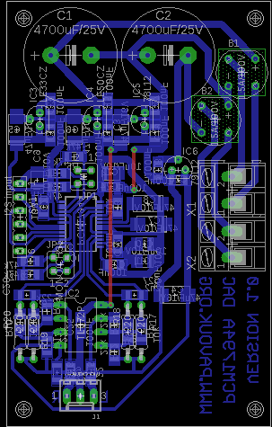
Printed circuit board is single sided with two wire connections, that it can be easily made in amateur conditions. Ground wires are drawed with accent to separating of digital and analog part. Decoupling capacitors are placed closely to DAC.
PCB of prototype on photos is a little different in these smallness: In schematics is additional pull-up resistor R5 on a reset signal. In datasheet is not discoverable that it must be used. SMD resistors and capacitors with size 0805 was replaced with 1206 size for easier mounting. I was succesful in reducing of wire connections from five to two.
Circuit is configured with 4 jumpers. When they are not installed, that they are pull-downed to zero with resistors. Setting of audio format is described next in the table. Most frequently I meet with I2S or right-justified 24bit format. If we connect board to our S/PDIF decoder, we must on them set identical data format and frequency of system clock. If we want to play 192kHz samples, we must set system clock maximally to 384 x fs. More informations are in a datasheet.
| PIN, JUMPER | Audio format | |||||
|---|---|---|---|---|---|---|
| MONO, JP2-1 | CHSL, JP2-2 | FMT1, JP1-2 | FMT0, JP1-1 | FORMAT | STEREO/MONO | DF ROLOFF |
| 0 | 0 | 0 | 0 | I2S | Stereo | Sharp |
| 0 | 0 | 0 | 1 | Left-justified | Stereo | Sharp |
| 0 | 0 | 1 | 0 | Right-justified 16bit | Stereo | Sharp |
| 0 | 0 | 1 | 1 | Right-justified 24bit | Stereo | Sharp |
| 0 | 1 | 0 | 0 | I2S | Stereo | Slow |
| 0 | 1 | 0 | 1 | Left-justified | Stereo | Slow |
| 0 | 1 | 1 | 0 | Right-justified 16bit | Stereo | Slow |
| 0 | 1 | 1 | 1 | Digital filter bypass | Mono | - |
| 1 | 0 | 0 | 0 | I2S | Mono, L-channel | Sharp |
| 1 | 0 | 0 | 1 | Left-justified | Mono, L-channel | Sharp |
| 1 | 0 | 1 | 0 | Right-justified 16bit | Mono, L-channel | Sharp |
| 1 | 0 | 1 | 1 | Right-justified 24bit | Mono, L-channel | Sharp |
| 1 | 1 | 0 | 0 | I2S | Mono, R-channel | Sharp |
| 1 | 1 | 0 | 1 | Left-justified | Mono, R-channel | Sharp |
| 1 | 1 | 1 | 0 | Right-justified 16bit | Mono, R-channel | Sharp |
| 1 | 1 | 1 | 1 | Right-justified 24bit | Mono, R-channel | Sharp |


| name | value and type | quantity |
|---|---|---|
| R1-R5 | 47k SMD1206 | 5x |
| R6-R10 | 10k SMD1206 | 5x |
| R11-R14 | 22k SMD 1206 | 4x |
| R15-R16 | 22R SMD 1206 | 2x |
| R17-R20 | 220R | 4x |
| C1-C2 | 4700uF/25V electrolytic | 2x |
| C3-C8 | 47uF/10V SMD tantal size C | 6x |
| C9-C12 | 10uF/10V SMD tantal size B | 4x |
| C13-C26 | 100nF SMD1206 ceramic | 14x |
| C27-C28 | 2n2 SMD1206 ceramic | 2x |
| IC1 | PCM1794A | 1x |
| IC2 | TL072 DIL8 | 1x |
| IC3 | LE33CZ TO92 | 1x |
| IC4 | LE50CZ TO92 | 1x |
| IC5 | 78L12 TO92 | 1x |
| IC6 | 79L12 TO92 | 1x |
| J1 | Molex 3pin | 1x |
| JP1-JP2 | JP2Q jumper | 2x |
| B1-B2 | Bridge rectifier 1.5A/100V round | 2x |
| SV1 | Jumper ribbon 6 pins | 1x |
| X1-X2 | Frame terminal AK300/2 | 2x |
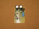
Audio DAC with PCM1794A has excellent parameters and sounds great. Traces on a scope looks very good too, but with high frequency 20kHz with sample frequency 44.1kHz we can see in a trace instead of "stairs" some smoothed connection with multiple traces. It is probably normal in a DAC with oversampling. My goal is to have DAC without oversampling which should guarantee high fidelity of playing. Circuit doesn't worked immediately for me. Reason was missing pull-up resistor on RESET signal. It could have insufficient description of reset function and incomplete schematics of circuit in a datasheet or my misunderstanding. For getting better parameters it is possible to try change operational amplifier TL072 with something better. We can completely bypass output amplifier and use symmetrical output before R7 to R10 resistors but only if we have high impedance input. Output from DAC is symmetrical around reference voltage and not around zero. Amplifier has symmetrical power supply and output has average value 0 voltage. We doesn't need to separate them with coupling capacitor. On the output can be a small d.c. voltage about few milivolts which is given by part value tolerance.
-
 English
 Česky
Česky