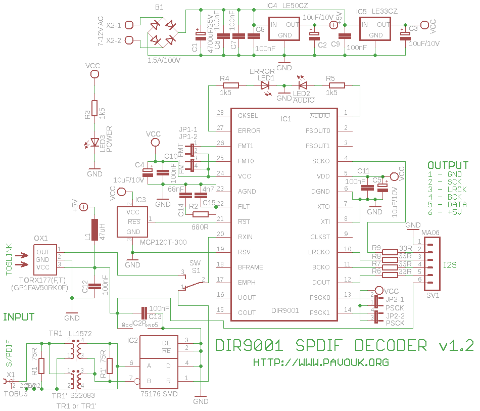
For transfer of digital audio between devices is standardized S/PDIF interface (electrical) and TOSLINK (optical) for commercial use, or AES3 for professional use. S/PDIF decoder module is used for converting of this interface to I2S interface, which is usually used on audio DACs. For conversion we can use for example integrated circuit CS8416 or DIR9001. In building of DAC in past I had troubles with resetting circuit CS8416 in hardware mode. Now I select DIR9001 which works perfectly and he has lower jitter than CS8416.
In supply section after bridge rectifier and smoothing capacitor I use LOW-DROP voltage regulators IC4 LE50CZ and IC5 LE33CZ. On optical input is used optical receiver OX1 Toshiba TORX173 with TTL output. On electrical input due to galvanic isolation is used pulse transformer TR1 and after him RS485 transceiver IC2 75176 with TTL output. I had better signal shape with termination resistor 75R connected before transformer. For isolation is possible to use transformer Lundahl LL1572, Newava S22083 or similar. Circuit board is prepared for both usual pinouts. When we doesn't need both types of input interface, we can wire in only one which we want. Components from second input we don't need. Circuit DIR9001 requires external reset circuit. I used available MCP120T-300. Circuit DIR9001 can use clocks from crystal or from input signal. I used circuit with internal PLL without external clocks which accept input signal with sample frequency 32, 44.1, 48, 88.2 and 96kHz. Internal PLL requires external filter composed from R2, C14 and C15. Output signals GND, SCK, LRCK, BCK, DATA and +5V goes to six pin connector which is dedicated for connecting of DAC board. POWER LED lights when power voltage is present. ERROR LED lights when S/PDIF signal is not present or when error is detected. _AUDIO LED lights when received S/PDIF signal doesn't contains RAW PCM audio data. For example when AC3 or DTS encoded signal is received.
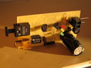
We must place components on board from smaller to bigger. First we must place IC1 which is really small. First I soldered two end pins and check the right position of circuit. Next I solder all pins with soldering iron and pipe tin. Almost all pins was now shorted. Next I exhaust superfluous tin with solder wick which is perfect for this work. I visually check PCB connection on my reading-lamp. Next I continued with placing of SMD resistors, capacitors, diodes and IC2. I continued with wire connections and components from a top side. When we doesn't need optical input, we doesn't place OX1 and C12. When we don't want electrical input, we don't place X1, R1, TR1, IC2 and C13.
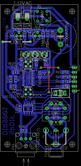
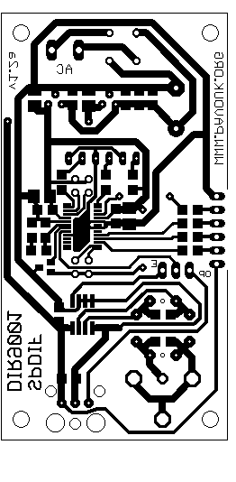
Printed circuit board is designed with only one side and two wire connections. It allows to create him in amateur conditions.
Output data format is selected by jumpers JP1-1 and JP1-2 connected to FMT0 and FMT1 pins. Next two jumpers JP2-1 and JP2-2 connected to PSCK0 and PSCK1 pins are for selecting of System clock. This is needed in respect to possibilities of DAC with oversampling. Circuit has internal pull-down resistors 51k. When jumper is not connected there is logical level L. When is connected, there is logical level H. We must set right output format in respect to used DAC. Next tables presents settings overview.
| FMT[1:0] settings | Audio data output format | |
|---|---|---|
| FMT1 | FMT0 | |
| L | L | 16-bit, MSB-first, right-justified |
| L | H | 24-bit, MSB-first, right-justified |
| H | L | 24-bit, MSB-first, left-justified |
| H | H | 24-bit, MSB-first, I2S |
| PSCK[1:0] settings | Output clock from PLL | |||
|---|---|---|---|---|
| PSCK1 | PSCK0 | SCKO | BCKO | LRCKO |
| L | L | 128fs | 64fs | fs |
| L | H | 256fs | 64fs | fs |
| H | L | 384fs | 64fs | fs |
| H | H | 512fs | 64fs | fs |


| name | value and type | quantity |
|---|---|---|
| R1 | 75R SMD1206 | 1x |
| R2 | 680R SMD1206 | 1x |
| R3-R5 | 1k5 SMD1206 | 3x |
| R6-R9 | 33R SMD1206 | 4x |
| C1 | 4700uF/25V electrolytic | 1x |
| C2-C5 | 10uF/10V SMD tantal size B | 4x |
| C6-C13 | 100nF SMD1206 ceramic | 8x |
| C14 | 68nF SMD1206 ceramic | 1x |
| C15 | 4n7 SMD1206 ceramic | 1x |
| IC1 | DIR9001 TSSOP28 | 1x |
| IC2 | 75176 SMD SO-08 | 1x |
| IC3 | MCP120T-300 SOT23 | 1x |
| IC4 | LE50CZ | 1x |
| IC5 | LE33CZ | 1x |
| JP1-JP2 | JP2QE jumper | 2x |
| L1 | 47uH axial | 1x |
| LED1 | LED red 2mA | 1x |
| LED2 | LED yellow 2mA | 1x |
| LED3 | LED green 2mA | 1x |
| B1 | Bridge rectifier 1.5A/100V | 1x |
| OX1 | TORX173 Toshiba - board 1.0 | 1x |
| OX1 | TORX177 Toshiba or GP1FAV50RK0F Sharp - board 1.2 | 1x |
| SV1 | jumper ribbon 6 pins | 1x |
| TR1 | LL1572 or S22083 or PE-65612 or DA102C | 1x |
| X1 | cinch female to PCB TOBU3 | 1x |
| X2 | frame terminal AK300/2 | 1x |
I hope that circuit doesn't have difficulties. We can have troubles with finding of circuit DIR9001 or pulse transformer which are not usually present in local store. Circuit works perfect for me and provides much variability in DAC bulding.
 English
 Česky
Česky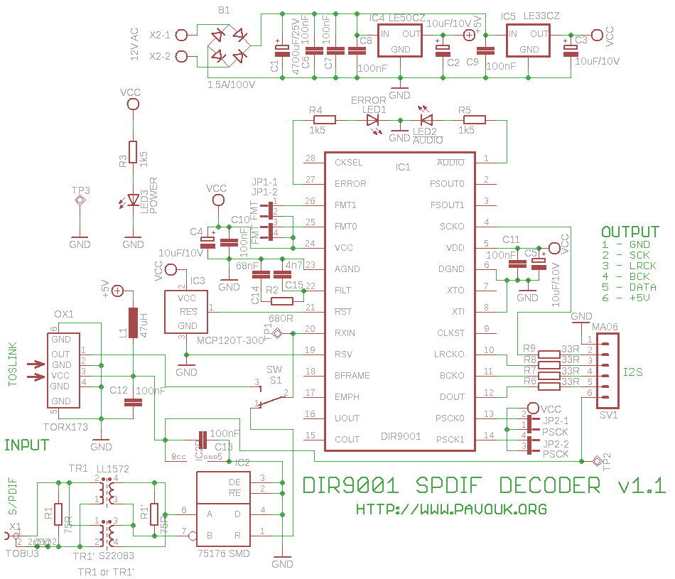