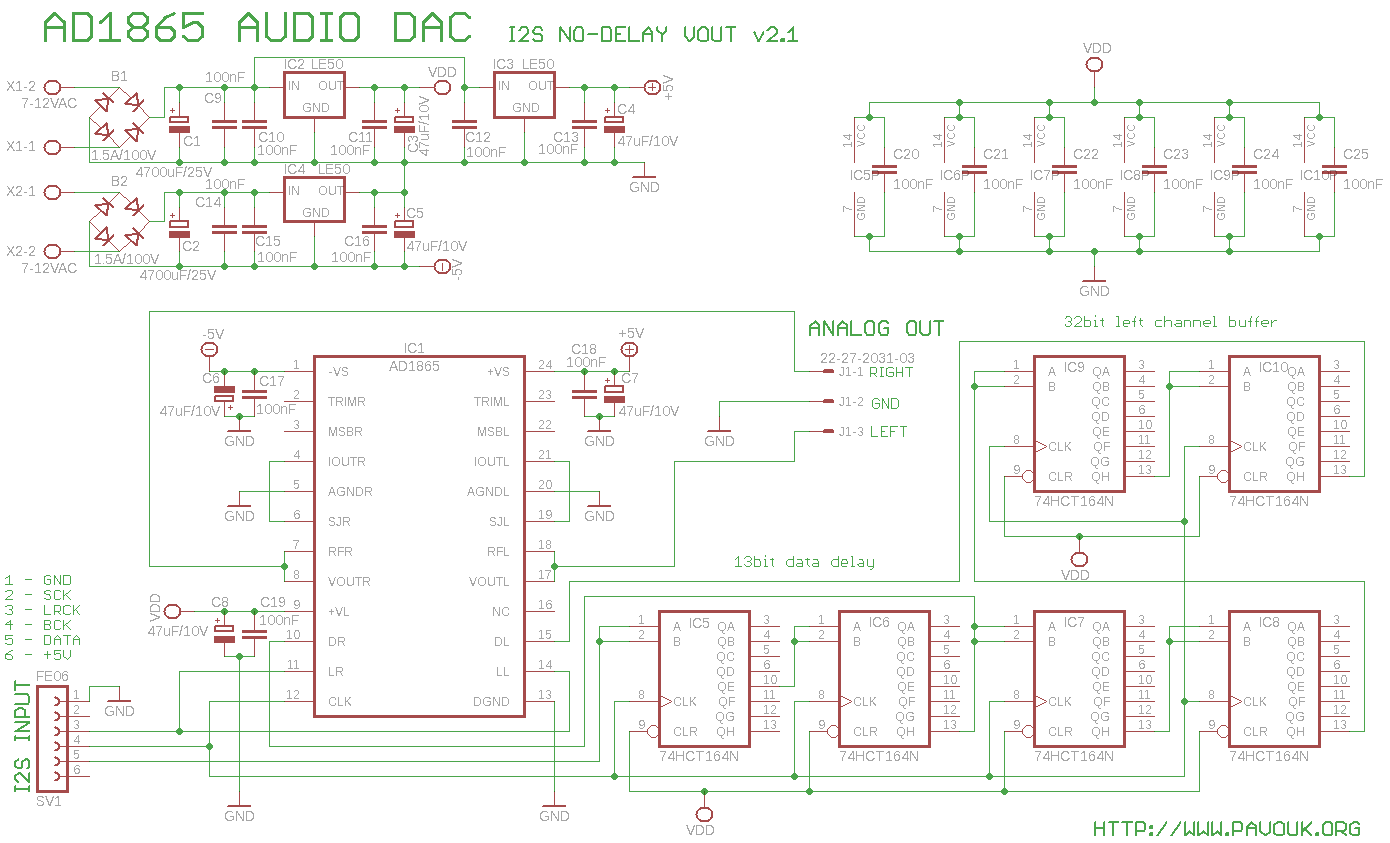
Circuit AD1865 is considered like best 18bit stereo audio DAC ever. I already built another DAC, that I will not say everything again. However I found, that current output is too weak and instead of using external I/V converter I used this, what is included in DAC. Because DAC doesn't have buffer for data, that both channels was not on the output simultaneously, but alternately left and right channel. This can produce theoretically hearable phase-shift. Last I want to connect DAC to USB receiver with only I2S data output. All troubles solve following circuit.
Supplying need two separated windings on power transformer, because I used positive voltage regulator for negative supply branch. After rectifiers B1 and B2 are filter capacitors C1 and C2 and behind them group of block capacitors. I used available low-drop voltage regulators LE50. One is for supplying of digital part and two are for positive and negative analog part of dac. Closely to regulators and integrated circuits are small filter and blocking capacitors.
DAC doesn't have I2S input, which is usual. It has individual data inputs for left and right channel and individual "latch" inputs which rewrites data from internal register to DAC output. Input data in I2S format (left justified) are first delayed for 13 bits thus that after shifting of 18 most significant bits to the dac register they will be written to output. For simultaneous playing of left and right channel we must delay data of left channel for 32 clocks (frame lenght for one channel). Result is that data for left and right channel are shifted together to the dac and they are written to the output with common latch signal. Because there doesn't exists 32bit shift-register I had two choices. Create them with help of Xilinx, but I have not experience with it or assemble them from easily available 8bit shift-registers. I wanted to avoid variant with registers train. However prototype with CMOS 64bit register CD4517 doesn't work thanks to different logic levels. On the end I had to use plenty of 74HCT164 which have 13 bits delay function and 32 bit register for left channel data. Result exceeded my expectations and DAC is fully functional for signals up to 192kHz/24bit which is 12.288MHz clock frequency.
This time I choose voltage DAC output. Output has +/-3V at maximum deflection which must be enough for every amplifier. In rest is zero on the output. Respectively there can be small DC offset few milivolts. Output can be direct-current separated with high quality capacitor if offset matter. There are no one filter on the output limiting frequency. I count with filtering in next parts of audio chain like amplifier, speaker and ear.
 schematics if I2S version in Eagle 5 format
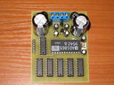
We assemble PCB from smaller parts to bigger. We begins with SMD capacitors and next with wire wraps. Circuits we can solder with small soldering iron and small 0.5mm tube tin. In case of emergency we can use transformer soldering iron and bigger tin. When some of pads will be connected together, we can exhaust overflowing tin with solder wick. Next I installed IC5 to IC10 and small capacitors from top side and next voltage regulators, connectors, rectifiers, dac and last big capacitors.
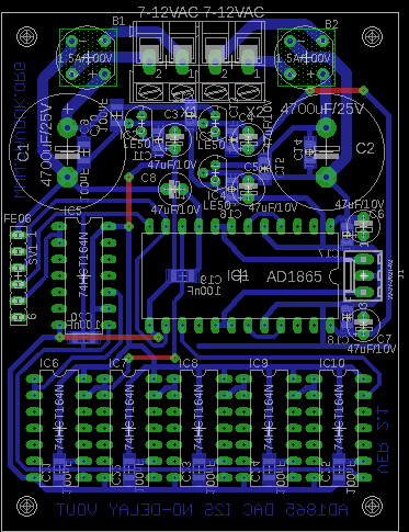
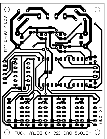
PCB is designed single sided with four wire junctions. It help as to make them in amateur conditions. SMD parts are from a bottom side and parts with wires and connectors are from a top side. Supply wires are designed with accent on right ground wiring and junction of analog and digital ground in a one point. Block capacitors are very close to circuits. PCB has four assembling holes for mounting with screws. Design of this board was this time difficult thanks to big number of parts, but finally all components was on the pretty small board with only four wire connections. After build of DAC I had to slightly modify board, because there was small digital noise visible on oscilloscope on one of the analog outputs. Now there are ground trace between digital and analog traces.


SMD capacitor have 1206 size which help with soldering. Circuits 74HCT164 are in DIL14 package for easy creating of PCB. They can be replaced with HC or ACT types. Other components with classic terminals are from the top. Except AD1865 circuit, which I bought on EBay are all components commonly available.
| name | value and type | quantity |
|---|---|---|
| C1, C2 | 4700uF/25V elektrolytic | 2x |
| C3-C8 | 47uF/10V low ESR elektrolytic RM2.5 | 6x |
| C9-C25 | 100nF SMD1206 ceramic | 17x |
| IC1 | AD1865 | 1x |
| IC2-IC4 | LE50 | 3x |
| IC5-IC10 | 74HCT164 DIL14 | 6x |
| J1 | Molex 3pin | 1x |
| B1, B2 | Bridge rectifier 1.5A/100V | 2x |
| SV1 | Jumper ribbon 6 pins | 1x |
| X1, X2 | Frame terminal AK300/2 | 2x |
First I built board with CD4517 shift-register. When I discovered that it doesn't work I had to create board with plenty of bugs. When board was finished and board works for CD quality, that I get idea to test FLACs with 192kHz/24bit sample frequency and I was very surprised that it works nicely without any issues. For this sample frequency we must use S/PDIF decoder based on CS8416, because DIR9001 support sample frequency up to 96kHz/24bit. We must use electrical S/PDIF input, because optical receiver TORX173 is too slow. It will be resolved with new generation of receivers TORX177, but about this perhaps next time :-)
-
 English
 Česky
Česky